  |
|
The Nixie Tube Propeller Clock has spun
times since midnight!
|
|
|||||||
| Nori Clock Hardware | |||||||
|
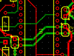
The ReworkThe main priority of this project was to make as much use of the existing PCMF hardware as possible, minimizing the amount of necessary modifications to the circuit board. Click the tile below to view the Nori Clock's schematic diagram in PDF format.
Physical changes:
Repurposed components:
Abandoned components:
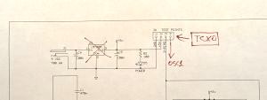
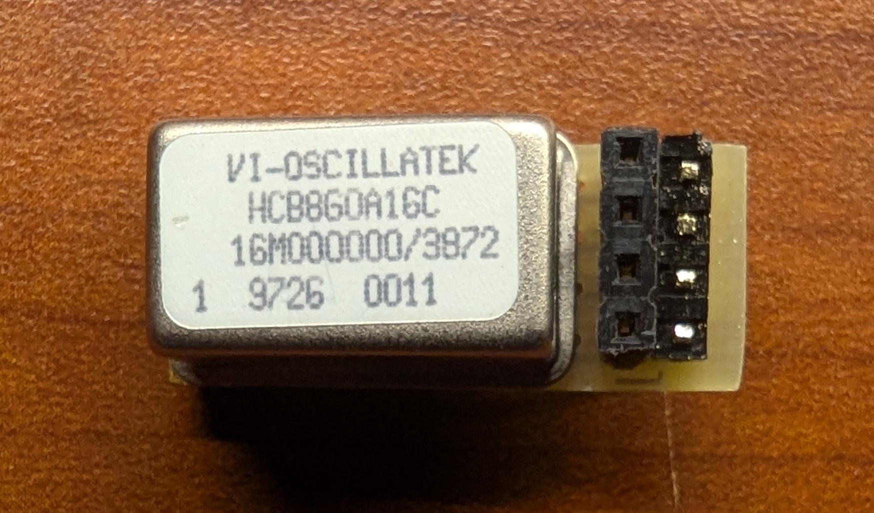
Power SupplyIn the days of the PCMF, small but powerful 5 V DC switching-mode power supplies were not at all ubiquitous, unlike today, in the age of USB chargers. This gave me the idea to utilize one of those for the Nori Clock instead of the 9 V wall wart, particularly because since the display is now always on, the 7805 linear regulator would be under constant heat stress. So I ended up popping the 7805 out of the PCB and power the device directly from an Apple charger cube through a USB-to-power-jack cable. GPIO's & the Infamous SPI SDIThe original PCMF design did not follow the well-vetted practices for unused GPIO's, which were left as floating inputs. While it did not cause any observable issues throughout the years, I found it appropriate to remedy this in the Nori Clock, by configuring them as low-driven outputs in the firmware. The only fly in the ointment was the MCU's RC4/SDI pin for the SPI SDI signal, which the SPI module configures as input, but the VFD offers nothing to feed it from. Because of this, the pin is now set up as input right after boot, while on the PCB it got connected to ground. One may assume that this part of the story was over, but that was far from the case. Having done the "right thing" with the GPIO's, a totally unexpected curveball appeared out of the blue for me. After receiving the PCMF's proto-1 PCB from fab back then, Monica and I noticed that one of the traces were too close to the MCU's RD1 pin, which we corrected in the follow-up design. Because I kept the P1 device and Monica got the final product, my specimen had this vulnerability all along - and alas, as I learned this time, after soldering there was indeed a short between the trace and the MCU pin. In the PCMF it did not cause any issues, but now with the unused GPIO's driven low, the short suddenly reared its ugly head. As luck would have it, the offending trace carries the VFD's SBUSY signal, with the short resulting in severely corrupted printouts, as the VFD's pleas for pause got silenced. This was a real head-scratcher, but after root-causing the issue and configuring the [unused] RD1 as input, normalcy returned. Clocking the Clock ProperlyAs it is explained on the PCMF Hardware page, the lack of need for precise time-keeping allowed us to use the MCU's internal oscillator in the design - but that just won't cut it for a decent clock! While the oscillator's deviation from the nominal 8 MHz can be compensated for via firmware, its temperature-dependence and long-term drift can undermine the clock's accuracy. Thanks to the charitable donation from a friend, I had a couple of 16 MHz 1 PPM TCXO (temperature-compensated crystal oscillator) modules lying around. Serendipitously, the PCMF's J4 debug header already had GND and +5V brought out, and also had an unconnected extra pin available - having wired that to the MCU's external clock input, the TCXO could now be attached to the circuit on a daughter board I fashioned, without disturbing the original PCB.
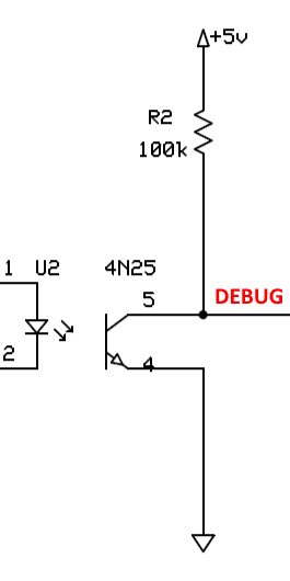
With frequency measurements and long-term monitoring of time-keeping I found that this TCXO provided perfect accuracy when its frequency adjustment pin was tied to ground, as opposed to being left floating. DEBUG SignalOn the PCMF, the J4:3 debug header pin carried the signal representing the ring pulses, as picked up by the optocoupler; this helped Monica fine-tune the ring detector circuit. Obviously the Nori Clock no longer has any use for this functionality, so the signal's RC2 GPIO (formerly input) got repurposed as the DEBUG output. This change of direction does not bother the now-defunct optocoupler; however this line also has a pull-up resistor to +5V, therefore I paid special attention that the signal is mostly driven high.
How the firmware utilizes the DEBUG signal is described here.
|
||||||


|

